Printable Die Attach Adhesives for Substarte-On-Chip Packaging
Printable Die Attach Adhesives for Substarte-On-Chip Packaging
Company:
Year:
Article keywords:
Abstract:
The dominant trend in packaging DDR DRAM for the future is the face down substrate-on-chip configuration. For this type of package it is critical that the die attach method employed provide precise control of bond line thickness and die tilt, minimal fillet, and prevent contamination of the wire bond pads located on the edge of the center wire bond channel. To date, a film adhesive has been the die attach method of choice because it is well suited to meet those requirements. Unfortunately, films are quite expensive compared to die attach pastes in terms of material, process, and tooling costs. This is especially true when changes such as die shrinks and board redesigns mandate a taping tool change. To address this serious issue, a novel series of printable B-stage adhesives has been developed that deliver the performance of a film (with respect to bond line and flow control), with the low cost of a paste (in terms of tooling and materials).
Type of document:
Language:
Printable Die Attach Adhesives for Substrate-On-Chip Packaging
Dr. Kevin Becker
Ablestik
Rancho Dominguez, CA, USA
kevin.becker@ablestik.com
Timmy Lin
ChipMOS Technologies
Hsinchu, Taiwan, Republic of China
ABSTRACT
The dominant trend in packaging DDR DRAM for the
future is the face down substrate-on-chip configuration. For
this type of package it is critical that the die attach method
employed provide precise control of bond line thickness and
die tilt, minimal fillet, and prevent contamination of the wire
bond pads located on the edge of the center wire bond
channel. To date, a film adhesive has been the die attach
method of choice because it is well suited to meet those
requirements. Unfortunately, films are quite expensive
compared to die attach pastes in terms of material, process,
and tooling costs. This is especially true when changes such
as die shrinks and board redesigns mandate a taping tool
change. To address this serious issue, a novel series of
printable B-stage adhesives has been developed that deliver
the performance of a film (with respect to bond line and
flow control), with the low cost of a paste (in terms of
tooling and materials).
In this paper, we will present data on a commercial series
and a developmental series of printable adhesives, which
were developed specifically for substrate-on-chip packages.
These proprietary adhesives are formulated to be stencil
printed on a substrate and then B-staged. The printed
substrates then replace the standard pre-taped substrates that
represent the mainstream in DRAM packaging. Data show
that these printable adhesives deliver the performance of
films, i.e. low flow and bond-line control on die attach,
more than a six month storage life at room temperature, and
do not require substrate pre-drying.
ChipMOS
Technologies has pioneered the assembly process using
these adhesives and are seeing high UPH and equivalent
reliability performance to film adhesives. Key in-package
reliability data from those evaluations will be presented.
Key Words: die attach, stencil print, adhesive, packaging
INTRODUCTION
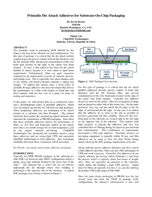
Typically the DDR DRAM packages in the substrate-onchip (SOC) or board-on-chip (BOC) configuration utilize a
plastic array type substrate bonded to the active face of the
chip1,2. The substrate has a center slot cut out directly
underneath the die through which wire bonding is
performed to the opposite side of the substrate. A typical
SOC package cross-section is shown in Figure 1.
Figure 1. SOC Package Cross-Section
For this type of package it is critical that the die attach
method employed provide precise control of bond line
thickness and die tilt, minimal fillet, and prevent
contamination of the wire bond pads located on the edge of
the center wire bond channel. Typically two adhesive
decals are used for die attach. They are rectangular in shape
and are placed on either side of the center slot. On the outer
perimeter, they may end just inside the die edge, at the die
edge, or just beyond the die edge. In any case, it is critical
that the adhesive be as close to the slot as possible to
prevent a gap being left after molding. However, the wirebond pads on the substrate are located right at the slot edge
on the opposite side of the substrate. This requires both
high accuracy in placing the adhesive, and very low
controlled flow or filleting during die attach to prevent bond
pad contamination. This combination of requirements
necessitates a film type adhesive. Punching accuracy on
pre-taping equipment is typically within 50 µm, and film
adhesives can be made to flow less than 50 µm during
attach, allowing the SOC package requirements to be met.
Along with the precise adhesive thickness and flow control
a film adhesive provides, films can also offer advantages in
UPH and work in process. Generally, film adhesives do not
require substrate pre-drying, which eliminates a step from
the process which is typically about four hours in length.
Also, films are generally pre-attached to the substrate,
which makes die bonding a high UPH process. Attach
times for films are typically less than 1 sec. per die enabling
die bonder UPH in the range of 500-2000.
Since the main stream packaging in DRAM over the last
several years has been the TSOP II package (LOC
configuration), the industry's infrastructure is also well
suited to the SOC package using film adhesives, as the
process is quite similar and the equipment used can be the
same.
Film die attach adhesives generally have the two drawbacks
of cost and voiding. On the performance side, films tend to
void either during attach or during cure, in no small part
because they are usually unfilled. This means that compared
to paste adhesives which are heavily filled with low
moisture absorbing particles, the moisture absorption is
significantly higher which can make the adhesive more
prone to voiding. While current reliability requirements in
the memory industry are usually only JEDEC Level 3, with
220-240ºC reflow (lower than for other packaging sectors),
voids in the bond line can cause failures in reliability testing
for almost any adhesive.
With respect to cost, film adhesive material cost tends to be
several times higher than for a typical paste adhesive. Even
more importantly, tooling costs for films are a significant
part of the total package cost, especially when die shrinks,
substrate redesigns, or R&D demands frequent tooling
changes. Punching tools for taping adhesive to substrate
can run several thousand dollars per machine, and typically
a similar number of taping machines is required as there are
die bonders, since UPH on the two processes are similar.
This can mean that a cost of several hundred thousand
dollars is incurred each time the tape decal is changed.
Nevertheless, to date film adhesives have been used almost
exclusively for SOC packaging, as they have been the only
readily available die attach adhesives suited to the package
demands. However, the cost-driven nature of the memory
packaging industry has created a demand for a lower total
cost solution to SOC packaging. This paper presents data
on a novel series of printable B-stage adhesives that deliver
the performance of a film (with respect to bond line and
flow control), with the low total cost of a paste (in terms of
tooling and materials).
3.0 Printable SOC Die Attach Adhesives
Printable die attach adhesives are used very similarly to film
adhesives except in the application method initially
employed to introduce the adhesive onto the substrate. The
general process flow is shown in Figure 2. In the case of a
printable adhesive, the material is stenciled onto the
substrate. A subsequent oven B-stage process will reduce
the adhesive thickness by removing the solvent leaving only
solid adhesive resins behind. At this point, there is no
difference in either physical make up or performance
between this material and a film adhesive.
3.1 Material Selection
Several adhesives are discussed in this paper. Each material
has been designed with particular process considerations in
mind. The main processing factors that will determine the
appropriate material selection are:
• the type of die bonder available (LOC, flip chip or
other),
• the stencil printing site (printing at the assembly house
or at the substrate manufacturer),
• whether the die bonding process is magazine-tomagazine or stack-to-magazine, and
• the amount of flow allowable or desired during die
attach.
Specifically, four adhesives will be discussed. Their
properties while in paste form are shown in Table 1.
Paste Properties
Com A
Filler Type
Chemistry
Solvent
Viscosity
(25ºC / 5 rpm)
Figure 2. Process Flow Comparison for Printable and Film
Die Attach Adhesives
Thixotropic
Index
Estimated
Work Life
(25ºC)
Open Time
( 20N (2 kgf) per die in order to be
well within the control range of the equipment. At the same
time, the SOC package geometry typically restricts flow
during attach, or filleting, to 7x12 mm) due to its
higher modulus.
All of these adhesives should be cured for 1 hr. @ 175ºC to
achieve full curing. A 30 minute ramp up time is
recommended in order to ensure minimal voiding, though
these materials are not prone to increased voiding during die
attach cure. Some or all of this cure time may coincide with
170ºC
160ºC
150ºC
140ºC
Poor wet-out
Recommended Process Window
Excessive Flow or Voiding
Figure 4. Die Attach Process Window for Dev A
Properties of the adhesives in their final cured state are
shown in Table 4. All these materials have high adhesion
strength, especially at elevated temperatures that simulate
solder reflow conditions. They also have low ionic impurity
levels, which is critical since they are being attached to the
active surface of the Si die. The low glass transition
temperature of these adhesives makes them tough,
compliant materials throughout the range of use and
processing temperatures. Their coefficients of thermal
expansion are somewhat lower than for typical epoxy
adhesives, resulting in relatively low package stress. Also,
the moisture resistance is very good. Com A, for example,
retains 75% of its room temperature adhesion strength after
48 hr. exposure to 85ºC, 85% RH, and 65% of its adhesion
strength at 245ºC. All these properties contribute to the
140ºC
150ºC
160ºC
170ºC
130ºC
120ºC
Die Size 7 x 7 mm – 1 sec. attach time used in all cases
Temp vs.
0.50
0.75
1.0 kg 1.5 kg 2.0 kg 2.5 kg
Force
kg
kg
% Voids
0%
0%
0%
0%
% Flow
0%
0%
< 1%
< 3%
%Wet80%
85%
90%
95%
out
% Voids
0%
0%
0%
0%
% Flow
< 1%
< 3%
< 5%
8%
% Wet95%
100%
100%
100%
out
% Voids
0%
0%
0%
% Flow
< 1%
< 3%
8%
% Wet95%
100%
100%
out
% Voids
0%
0%
0%
0%
0%
% Flow < 1% < 1%
< 3%
5%
10%
% Wet8095%
100%
100%
100%
out
90%
% Voids
0%
< 1%
< 1%
< 1%
% Flow < 1% < 3%
5%
15%
% Wet90%
100%
100%
100%
out
% Voids
0%
0%
< 1%
< 1%
% Flow < 1% < 1%
5%
15%
% Wet90%
95%
100%
100%
out
outstanding reliability performance exhibited by this series
of adhesives.
180ºC
the post-mold curing, depending on process demands after
die attach. Also, lower curing temperatures may work,
again depending on process demands on the die attach
material. The cure schedule needs to be optimized on an
individual basis depending on process, package geometry
and warpage considerations.
Die Size 7 x 7 mm – 1 sec. attach time used in all cases
Temp vs.
1.5 kg 2.0 kg 2.5 kg 3.0 kg 3.5 kg
Force
% Voids
0%
0%
% Flow
0%
< 3%
% Wet-out
50%
90%
% Voids
0%
0%
0%
% Flow
0%
0%
< 3%
% Wet-out
50%
75%
90%
100%
% Voids
0%
0%
0%
0%
% Flow
0%
0%
< 2%
< 5%
% Wet-out
60%
90%
95%
100%
% Voids
0%
0%
0%
< 3%
% Flow
0%
< 2%
< 5%
< 10%
% Wet-out
80%
90%
95%
100%
% Voids
0%
0%
0%
0%
0%
% Flow
0%
0%
< 3%
< 5%
< 10%
% Wet-out
90%
95%
100%
100%
100%
Poor wet-out
Recommended Process Window
Excessive Flow or Voiding
Figure 5. Die Attach Process Window for Dev B
3.5 Package Reliability:
These printable adhesives have shown excellent reliability
performance to date. The current MRT standard for most
memory devices is JEDEC Level 3 with a reflow
temperature of either 220ºC or 240ºC. However, most new
packages are being qualified at Level 3, 260ºC reflow in
order to meet Pb-free packaging requirements. Com A series
and the developmental series adhesives have been shown
not only to meet, but exceed this standard. ChipMOS
Technologies has qualified Com A on several DRAM
devices at JEDEC Level 3/220ºC. Additionally, they have
tested package reliability at Level 3/260ºC and at Level
2/220ºC on their SOC 60B 256Mb SDRAM package and
both tests passed. Higher reliability has not been tested at
ChipMOS. Results of the Level 3, 260 test are shown in
Figure 6. Elsewhere, Dev A has passed JEDEC Level
2/260ºC reflow, and Dev B has passed JEDEC Level
3/245ºC reflow on similar packages. Again, no higher
reliability levels were tested.
No delamination is observed after preconditioning and
solder reflow
Properties After Cure
Com A
Die
Shear
Strength
2x2
mm die
(kg/cm2)
Tg
CTE
(ppm/ºC)
Dev C
4
4
2
1
K
N/D*
N/D*
N/D*
N/D*
Cl
Dynamic
Tensile
Modulus
(MPa)
Dev B
Na
Ionics
(ppm)
Dev A
13
12
9
5
25ºC
950
1100
1600
2100
150ºC
20
53
130
160
250ºC
9.7
15
24
21
25ºC
245ºC
463
73
535
78
453
63
575
100
TMA
-10ºC
-16ºC
67ºC
17ºC
Below
Tg
94
72
83
58
Above
Tg
237
187
205
139
Table 4. Typical Stencil Print Adhesive Properties After
Cure
• N/D = value is below the detectable limit (~1ppm)
ChipMOS Technologies' SOC 60B 128Mb and 256Mb
SDRAM packages have also passed the following reliability
tests:
1000 hours High
Temperature
Storage
1000 hours
Temperature,
Humidity, Bias
240 hours
Pressure Cooker
Test
1000 cycle
Thermal Cycle
Test
100 hours Highly
Accelerated
Stress Test
150ºC
THB
85ºC / 85% RH /
3.6V
PCT
121ºC / 100% RH /
2 atm
TCT
-65ºC to + 150ºC
in air
HAST
130ºC / 85 RH /
3.6V
4.0 Conclusions
New novel printable adhesives have been developed to
replace traditional film adhesives for low cost SOC-type
memory packaging.
These commercial series and
developmental series adhesives are printed onto the
substrate and then oven B-staged to provide substrates with
pre-applied adhesive for DRAM packaging. The adhesives
provide at least equivalent performance to commercially
available films at every process step and in package
reliability. Significant savings can be realized by using such
adhesives through lower material costs and lower process
and tooling costs. The adhesives have been designed to fit
the existing packaging infrastructure for main stream
DRAM device manufacture. Com A is now qualified at
ChipMOS on various SDRAM and DDR DRAM devices
and is in mass production.
5.0
1)
2)
3)
Figure 6. JEDEC Level 3 with 260ºC Reflow Reliability
Results for ChipMOS' SOC 60B 256Mb SDRAM Package
HTS
References
US Patent # 6048755; Issued to Micron in 2000
TW Patent # 447094; Issued to ChipMOS in 2001
US Patent Application # 10/016,844; Submitted by
Ablestik
Coments go here:
- Log in to post comments